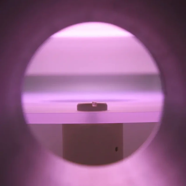
Introduction to PECVD and its Significance
Plasma-Enhanced Chemical Vapor Deposition (PECVD) is a process that deposits thin films of materials such as silicon oxide, silicon nitride, and amorphous silicon onto a substrate. This technique is widely used in the semiconductor industry for creating microelectronic devices such as transistors, capacitors, and interconnects. PECVD offers several advantages over traditional CVD, such as lower processing temperatures, higher deposition rates, and better film quality. With the increasing demand for advanced microelectronic devices, the PECVD market is expected to grow significantly in the coming years.
Table of Contents
- Introduction to PECVD and its Significance
- How PECVD Deposition is Achieved
- Factors driving demand in the PECVD market
- Global Segmentation of the PECVD Systems Market
- Applications of PECVD in Semiconductor Manufacturing
- Benefits of PECVD over traditional CVD
- The Role of Plasma in PECVD
- Empirical Improvements for PECVD
How PECVD Deposition is Achieved
PECVD is a plasma-enhanced chemical vapor deposition process that is widely used in the production of thin films for various applications. The PECVD process involves depositing thin films by introducing a gas mixture of the desired material into a vacuum chamber, where it is ionized by a plasma discharge. In this section, we will discuss step by step how PECVD deposition is achieved.

Step 1: Preparation of the Substrate
The first step in the PECVD process is the preparation of the substrate. The substrate is typically made of silicon, and it is cleaned thoroughly to remove any impurities from the surface. The substrate is then placed in the vacuum chamber, where the deposition process will take place.
Step 2: Introduction of Precursor Gases
The second step is the introduction of precursor gases into the vacuum chamber. The precursor gases are typically a mixture of the desired material, such as silicon or silicon nitride. The gases are introduced into the vacuum chamber through a gas delivery system.
Step 3: Activation of Precursor Gases
The third step is the activation of the precursor gases. This is achieved by applying a high-frequency electric field to the gas mixture, which causes the gas molecules to ionize and break down into their constituent parts. The plasma discharge also heats up the substrate to a temperature that is suitable for the deposition process.
Step 4: Formation of Thin Film
The fourth step is the formation of the thin film. The precursor gases react with the surface of the substrate to form a thin film. The process is achieved by the plasma discharge, which causes the gas molecules to break down into their constituent parts and react with the surface of the substrate.
Step 5: Control of Film Properties
The final step is the control of the film properties. This is achieved by controlling the deposition parameters, such as gas flow rate, pressure, and temperature. By controlling these parameters, it is possible to achieve the desired film properties, such as thickness, uniformity, and composition.
In conclusion, PECVD deposition is achieved by preparing the substrate, introducing precursor gases, activating the precursor gases, forming the thin film, and controlling the film properties. The PECVD process is widely used in the semiconductor industry for the production of various thin films, including microelectronic components, solar cells, and sensors. Understanding the PECVD method and how it is achieved is important for those working in the field of laboratory equipment, as it is an essential technique used in the production of many critical components and devices.
Factors driving demand in the PECVD market
The PECVD method is widely used in the semiconductor industry for its ability to deposit a variety of materials, including silicon dioxide, silicon nitride, and amorphous silicon. The PECVD process has several advantages, including uniformity, the ability to deposit on a variety of substrates, and excellent step coverage. These advantages have driven demand in the PECVD market and it is expected to grow at a CAGR of 7.4% from 2020 to 2027.
Increasing demand for semiconductors in various applications
The increasing demand for semiconductors in various applications, such as smartphones, tablets, and laptops, has been one of the primary drivers of demand in the PECVD market. The demand for electronic devices continues to grow, and PECVD systems are an essential tool in modern semiconductor manufacturing processes, offering excellent film uniformity, low-temperature processing, and high throughput.
Growing demand for renewable energy and electric vehicles
The growing demand for renewable energy and electric vehicles has led to an increase in demand for PECVD equipment to manufacture solar cells and lithium-ion batteries. Solar cells and lithium-ion batteries are essential components of renewable energy and electric vehicles, and the PECVD method is widely used in their production.
Development of new technologies
The PECVD market is also being driven by the development of new technologies, such as 5G. 5G is expected to increase the demand for PECVD equipment in the manufacturing of RF filters and other components. As the demand for advanced electronic devices continues to grow, PECVD systems will play an increasingly important role in the semiconductor industry.
High concentration of foundries and semiconductor manufacturers
The APAC region had the dominant share of the global PECVD systems market due to the high concentration of foundries, semiconductor wafer manufacturers, semiconductor memory device manufacturers, and IDMs. The North American region also dominates the PECVD market owing to the growing investments in autonomous vehicles, 5G networks, AI, smart lighting, electronic warfare equipment, and renewable energy sources. As the investments in the establishment of new fabs or fabrication plants continue to rise, the demand for PECVD systems has increased as they are used for substrate deposition.
In conclusion, the PECVD method is a crucial process in the semiconductor industry, and the growing demand for semiconductors in various applications, the increasing demand for renewable energy and electric vehicles, the development of new technologies, and the high concentration of foundries and semiconductor manufacturers are driving the demand for PECVD equipment in the market.
Global Segmentation of the PECVD Systems Market
The plasma-enhanced chemical vapor deposition (PECVD) method is a widely used technique in the manufacture of high-quality thin films for various applications, such as electronics, semiconductors, and solar cells. The PECVD systems market is expected to grow significantly in the coming years due to the increasing demand for thin films in various industries. The market is segmented into four main regions: North America, Europe, Asia Pacific, and Rest of World.
Factors Affecting the Segmentation
The market segmentation is based on various factors, including technology, product type, application, and geographical region. The technology segment includes plasma-enhanced CVD, atmospheric pressure CVD, and low-pressure CVD. The product type segment includes equipment, precursors, and services. The application segment includes semiconductor and microelectronics, photovoltaics, tribological, optical, and biomedical fields. The geographical region segment includes North America, Europe, Asia Pacific, and the Rest of World.
Market Value and Additional Market Segments
An analysis of the semiconductor and microelectronics industry alone shows that its annual revenue of precursors and chemicals for CVD and related methods of manufacturing thin films totaled $1.4 billion USD in 2020. To this market, bulk gases and chamber clean gases must be added. While this does not give a full picture of the number of molecules and energy consumed and waste generated by the semiconductor CVD industry, it gives a scale to the sector and a scope of the market growth when compared over time, and more importantly, the future growth of the CVD market.
The CVD films required in the cutting tools and drills sector are thicker than the films deposited in the semiconductor and microelectronics sector, leading to a higher consumption of chemicals and generation of waste. The sub-equipment market for CVD precursors delivery systems and containers, gas supply, process gas abatement, vacuum pumps, and other utilities needed for high volume production of CVD films corresponds to an additional market segment, and we estimate it to be 15-20% in annual revenue of the annual equipment market.
Applications of PECVD in Semiconductor Manufacturing
PECVD is a widely used method in the semiconductor manufacturing industry due to its ability to create thin films of various materials on a substrate, using plasma-enhanced chemical reactions. The PECVD method offers several advantages, one of which is the deposition of high-quality thin films at low temperatures. This is beneficial for semiconductor devices that are sensitive to high temperatures. PECVD is used to deposit a variety of materials such as silicon dioxide, silicon nitride, amorphous silicon, and diamond-like carbon. These materials have different applications in the semiconductor industry, including the following:
Interlayer Dielectrics
PECVD is used to create low dielectric constant (low-k) films for interlayer dielectrics. Interlayer dielectrics are used to isolate conductive layers in integrated circuits, preventing electrical interference between them. Low-k films have lower capacitance than silicon dioxide films, which reduces the signal delay time, and improves the performance of the integrated circuits.
Barrier Layers
Barrier layers are used to prevent diffusion of metal atoms into the surrounding material, which can cause degradation of the device performance. PECVD is used to create barrier layers for metallization. These barrier layers are usually made of silicon nitride or silicon carbide.
Surface Passivation
PECVD is used to create a passivation layer on the surface of semiconductor devices. The passivation layer serves as a protective layer, preventing the device from being damaged by external factors such as moisture and oxygen. The passivation layer can be made of silicon dioxide or silicon nitride.
Anti-Reflective Coatings
PECVD is used to create anti-reflective coatings on the surface of semiconductor devices. The anti-reflective coating reduces the amount of light that is reflected from the surface of the device, improving the accuracy of measurements during the fabrication process.
Solar Cells
PECVD is used to create thin films for solar cells. The thin films are used as anti-reflective coatings, passivation layers, and as the active layer in the solar cell. The active layer is usually made of amorphous silicon or microcrystalline silicon.
In conclusion, PECVD is an essential method in the semiconductor manufacturing industry. It is used to create thin films of various materials on a substrate, which have different applications in the industry. The deposition of high-quality thin films at low temperatures, with specific properties that are essential for the performance of semiconductor devices is an important advantage of the PECVD method. Understanding the applications of PECVD in semiconductor manufacturing is crucial for anyone working in the field of laboratory equipment.
Benefits of PECVD over traditional CVD
Lower Deposition Temperature
PECVD has a significant advantage over traditional CVD in that it operates at lower temperatures. While traditional CVD typically requires temperatures of 600°C to 800°C, PECVD can operate at a lower temperature range of room temperature to 350°C. This makes PECVD ideal for use in situations where higher temperatures could potentially damage the device or substrate being coated. By operating at a lower temperature, it creates less stress between thin film layers that have different thermal expansion/contraction coefficients. This allows for high-efficiency electrical performance and bonding to very high standards.
High Deposition Efficiency
PECVD offers high deposition efficiency compared to traditional CVD. This is because the reactions mainly take place on the cathode surface, which is beneficial to increase the deposition rate and reduce the loss of reactants on the wall of the deposition chamber. By optimizing parameters such as air pressure, temperature, discharge methods, discharge voltage, current density, and ventilation, it is possible to obtain more excellent compound thin-film materials.
Controllable Parameters
PECVD offers many controllable parameters compared to traditional CVD. In addition to air pressure and temperature, there are discharge methods, discharge voltage, current density, ventilation method, etc. By optimizing these parameters, it is practical to obtain more excellent compound thin-film materials.
Ability to Deposit on a Wide Range of Substrates
PECVD has an advantage over traditional CVD in that it can deposit thin films on a wider range of substrates, including plastics, glasses, and polymers. This is because the polyatomic gas discharge can lower the deposition temperature of compound films and expand the material range of substrates with compound film. For example, radiofrequency discharge and microwave discharge are suitable methods to produce a higher-density plasma at low temperatures.
Ability to Deposit a Wide Range of Materials
PECVD offers the ability to deposit a wide range of materials, including silicon dioxide, silicon nitride, and carbon-based materials. This makes it a highly versatile technique that can be used in a wide range of industrial and research applications.
Environmentally Friendly
PECVD is a more environmentally-friendly process compared to traditional CVD. This is because it uses less energy and produces fewer harmful by-products. By using a high-energy plasma to activate and accelerate the chemical reactions involved in the deposition process, PECVD results in a more uniform, high-quality film deposition with exceptional adhesion properties.
Overall, PECVD is a highly advanced and effective method for the deposition of thin films in a wide range of industrial and research applications. Its benefits over traditional CVD make it a preferred method for many laboratories and industries.
The Role of Plasma in PECVD
PECVD is a widely used process in the semiconductor industry for depositing thin films of various materials onto a substrate. The process involves the use of plasma, a gas made up of ions and electrons, that is used to break down the precursor gas molecules into reactive species, which then combine to form the desired thin film. The role of plasma in PECVD is crucial, as it provides the necessary energy to break the chemical bonds of the precursor gases, enabling them to react and form the desired film.
Plasma Activation of Reactants
Plasma enhanced chemical vapor deposition (PECVD) is a process technology whereby the activation energy for the CVD reaction to occur is achieved not just by temperature, but also by an energetic plasma formed in an electric (DC or RF) field. The plasma contains electrons and ions possessing energies that are able to break chemical bonds. Therefore, electron-molecule collisions create radicals in the gas phase and ions bombarding the surface of growing film activate the surface by creating dangling bonds. The ions also help to densify the growing film by etching weakly bonded terminating groups.
Control of Deposition Process
The plasma in PECVD also provides a way to control the deposition process, as the energy and density of the plasma can be manipulated to change the properties of the film being deposited. Different types of plasma sources, such as capacitively coupled plasma (CCP) and inductively coupled plasma (ICP), can be used to create plasma in PECVD, each with its own advantages and disadvantages. By varying the plasma, we can add additional control to the properties of the deposited film.
Low-Temperature Processing
PECVD technology uses low-temperature plasma to generate a glow discharge at the cathode of the process chamber under low air pressure. By using plasma to activate the reactants, PECVD can operate at lower temperatures than thermally driven CVD. In PECVD, the plasma is usually ignited and sustained by applying a high-frequency voltage to a low-pressure gas. In the plasma, inelastic collisions take place between electrons and gas molecules forming reactive species, such as excited neutrals and free radicals, as well as ions and electrons. In essence, the electrons acquire sufficient energy from the applied electric field to create highly reactive species without significantly raising the gas temperature.
In conclusion, understanding the role of plasma in PECVD is essential for optimizing the deposition process and achieving the desired film quality and properties. Plasma provides the necessary energy to break the chemical bonds of the precursor gases, enabling them to react and form the desired film. By manipulating the energy and density of the plasma, we can also control the deposition process and change the properties of the film being deposited. Overall, the PECVD method is a valuable tool for depositing thin films in a controlled and precise manner.
Empirical Improvements for PECVD
Thin film deposition using PECVD is widely used in various applications, including solar cell manufacturing, biomedical engineering, and the semiconductor industry. Despite its popularity, achieving high-quality, uniform films with good adhesion to the substrate remains a challenge. As such, empirical improvements have been made to address these challenges.
Process Optimization
One empirical improvement for PECVD is process optimization. Optimizing the process parameters such as temperature, pressure, gas flow rates, and power input can improve the quality of the film. This involves finding the right combination of process parameters that can produce high-quality films with good adhesion to the substrate.
Pre-treatment Steps
Another approach is to introduce a pre-treatment step, such as plasma cleaning or annealing, to improve the adhesion of the film to the substrate. Plasma cleaning can remove impurities and contaminants from the substrate surface before deposition. Annealing, on the other hand, can help to eliminate defects and improve the crystallinity of the deposited film.
Gas Mixtures and Precursors
Using different gas mixtures or precursors is also an empirical improvement for PECVD. By choosing the right gas mixture or precursor, the desired material properties can be achieved. For instance, adding hydrogen gas to the plasma can reduce stress in the film and improve its mechanical properties.
Multi-step Deposition Process
Lastly, using a multi-step deposition process, where different layers are deposited sequentially, can improve film quality and control thickness and composition. This approach allows for the growth of complex structures with precise control over layer thickness and composition.
In conclusion, empirical improvements for PECVD have contributed to the advancement of thin film deposition technology. These improvements include process optimization, pre-treatment steps, the use of different gas mixtures and precursors, and multi-step deposition processes. By employing these empirical improvements, high-quality, uniform films with good adhesion to the substrate can be achieved.
Produtos relacionados
- Sistema de Equipamento CVD de Deposição Química em Fase Vapor Câmara Deslizante Forno Tubular PECVD com Gaseificador de Líquidos Máquina PECVD
- Sistema RF PECVD Deposição Química de Vapor Aprimorada por Plasma de Radiofrequência RF PECVD
- Forno de Tubo de Deposição Química de Vapor Assistida por Plasma (PECVD) Rotativo Inclinado
- Equipamento de Deposição Química em Fase de Vapor Aprimorada por Plasma Rotativo Inclinado PECVD Forno Tubular
- 915MHz MPCVD Máquina de Diamante Sistema de Reator de Deposição Química de Vapor de Plasma de Micro-ondas
Artigos relacionados
- Comparação entre a deposição química de vapor e a deposição física de vapor
- Vantagens da deposição química de vapor
- Um guia completo para a manutenção de equipamento PECVD
- Exame aprofundado dos revestimentos por deposição química em fase vapor (CVD)
- Porque é que o PECVD é essencial para o fabrico de dispositivos microelectrónicos


